In a lithographic exposure tool, there is a glass mask which is fractional covered with chrome to partial expose areas of the resist.
Depending on the type of the resist, exposured areas are solubly or insolubly. With a wet-chemical developer the solubly parts are removed, so that a patterned resist layer remains. The exposure time is a very important value to achieve the correct dimensions of the structures. The longer the wafers are exposed to the radiation, the larger the radiated area is. Due to fluctuating ambient temperatures a precise determination of the correct exposure time has to be investigated with one or more dummy wafers, because the characteristics of the resist can change with temperature.
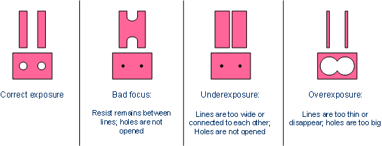
An overexposure causes smaller resist patterns, and therefore smaller structures beneath, in contrast vias will be enlarged. With a too short exposure time the vias are not opened correctly, conductors are to wide or even in contact to each other (short circuit). In addition, a bad focusing leads to unexposed areas, so that vias can not be opened and conductors are in contact as well.
Depending on the subsequent process, the width of the resist patterns or the diameter of the vias, respectively, has to be adjusted. In isotropic etch processes (etching in vertical and horizontal orientation) the resist mask is not transferred 1:1 into the layer beneath.